| HOME | CURRENT ISSUE | PHOTONICS RESOURCES | PRODUCTS | WEB EXCLUSIVES | LARRY'S VC VIEW BLOG | VIDEO | JOBS | EVENTS | LINKS |

 e-newsletter
 magazines


OPTOFLUIDICS: Nanolaser becomes a refractive-index sensor
Measuring the change in refractive index of a liquid induced by the entry of a foreign substance is one way to determine whether the liquid has become contaminated. The validity of this technique, however, depends on the accuracy of the refractive-index sensor. In addition, testing in the fieldsay, for example, pollution testingis easier with a sensor that is portable and relatively simple.
One approach to refractive-index sensing relies on a resonant optical cavity open to (or, if solid, somehow otherwise affected by) the liquid or gas under test; in this case, the resonant wavelength changes in proportion to the refractive index of the material in the cavity. A group of scientists at Yokohama National University (Yokohama, Japan) and Core Research for Evolutional Science and Technology (CREST), Japan Science Technology Agency (Tokyo, Japan) are using continuous-wave photonic-crystal nanolasers as the microcavities in two configurations: one, a single nanolaser in combination with a spectrometer; and two, an array of nanolasers, each slightly different, allowing for the fabrication of a very simple, spectrometer-free device.
Although an individual nanolaser in their device is formed as part of a hexagonal array of air holes in a single-quantum-well gallium indium arsenide phosphide (GaInAsP) wafer, it does not consist of the absence of a hole; instead, it is formed by the slight lateral shifting of four of the holes to create a nanocavity (see figure). The active layer of the wafer (including separate-confinement-heterostructure layers) is 180 nm thick. In a typical device, the air holes are 300 nm in diameter, the lattice spacing is 520 nm, the lateral (Sx) displacement of two of the holes is 120 nm, and the lateral (Sy) displacement of the other two holes is 60 nm. The GaInAsP wafer has a photoluminescence peak centered at about 1550 nm.
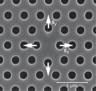
Four of the airholes in a hexagonal nanolattice in a GaInAsP single-quantum-well wafer are shiftedtwo laterally by 60 nm (Sx) and two longitudinally by 120 nm (Sy). The result is a nanolaser cavity that achieves continuous-wave lasing in the 1550 nm region when pumped by light at 980 nm. As the refractive index of the surrounding gas or fluid changes, the wavelength of the nanolaser changes, allowing monitoring of the index. (Courtesy of Yokohama National University and CREST)
The nanocavity is pumped by continuous-wave (CW) laser light at 980 nm focused to a 2.5 µm spot on the cavity, provoking the nanolaser itself to lase CW. The researchers chose CW operation for the nanolaser to avoid sensitivity-reducing line-broadening caused by thermal chirping. Depending on laser geometry, such a nanolaser exhibits either its fundamental cavity mode, or its fundamental mode plus a dipole mode. For stable sensing, the researchers decided to rely on lasers emitting only in the fundamental mode, for which they obtained lasing at refractive indices (of the surrounding liquid) between 1.00 and 1.37.
When used in combination with a spectrometer, the nanolaser achieved an index-sensing sensitivity of 250 to 300 nm/RIU in monopole mode (one RIU, or refractive-index unit, is equal to a refractive index change of one). If a homodyne or heterodyne type ultrahigh-resolution optical spectrum analyzer is available, 106 to 107 RIU is expected to be resolved by the CW nanolaser, says Toshihiko Baba, one of the researchers. Then, it could detect the small change induced by the approach of an environmental gas or liquid, approaching chemicals, biomolecules, and so on. Low cost, ease of disposal, and integration with microfluidics will be the keys for practical use.
Spectrometer-free operation
Another version dispenses with the spectrometer and has an array of nanolasers, each with slightly different cavity size; all are pumped and monitored simultaneously. For example, one thousand nanolasers fitted into a 340 × 340 µm sensor area with the separation between laser wavelengths equal to 20 pm would cover a refractive-index range of perhaps ±0.05 around some important point, at an index resolution of 104. One difficulty is controlling the nanocavity sizes to the needed resolution. Baba notes, however, that his groups electron-beam writing machine has a resolution of 1.25 nm. In addition, the wavelength shift is more sensitive to Sx and rather insensitive to Sy, says Baba. This means that these dimensions can be used for coarse and fine control.
As a test, the researchers fabricated an array of four nanolasers and modified their output with a bandpass filter (BPF) with a transmittance of 10%, 50%, and 90% at 1.534, 1.544, and 1.552 nm, respectively. When the lasers were immersed in the test medium, the BPF passed the light from none, one, two, or three of the lasers, respectively, as the refractive index of the test fluid changed from 1.325, to 1.344, to 1.363, to 1.420. Because this sort of device needs no spectrometer, wideband light source, or complex optical input and output, the researchers see its use for low-cost and disposable biochemical sensors; they also believe it will become part of lab-on-a-chip technology.
John Wallace
REFERENCE
1. Y. Yang et al., Applied Phys. Lett. 92, 163306 (2008).
Tue Jul 01 00:00:00 CDT 2008
Laser Focus World Article Categories:


featured webcasts


Vibration Control: Principles and Criteria for Isolation of Vibration-Sensitive Objects
Original broadcast on
2007/10/31


White Papers
|
|
Cleaning
Optics
(02/15/2008) Why
Use Edge Blackened Optics
(02/15/2008) Visual
Color Matching
(01/31/2008) Inside
Filters
(01/31/2008) Utilizing
Aspheres in Optical Design
(02/29/2008) |
White Paper Categories:
| Applications |
Detectors
and Imaging |
| Fiberoptics |
General |
| Instrumentation
and Accessories |
Lasers
and Sources |
| Optics |
7?, 2008


- Home |
- About Us |
- Contact Us |
- Site Map |
- Advertise
- Also visit: Industrial Laser Solutions |
- Vision Systems Design |
- Military & Aerospace Electronics |
- BioOptics World
- Copyright © 2007: PennWell Corporation, Tulsa, OK; All Rights Reserved. |
- Privacy Policy |
- Terms & Conditions