3D photonics
Photonic crystals optical analogues of
electronic semiconductors hold great promise for
manipulating and processing light signals in future
photonic devices. A new 3D microassembly technique could
greatly aid the development of photonic crystals for
such applications.
6 February 2003
Ed Gerstner
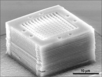 |
| Scanning electron micrograph of
one of the authors' 3D photonic crystal
structures. Multiple plates are patterned using
standard lithographic and etching techniques,
and then assembled into a stack using fine
mechanical probes. | |
 |
The tremendous progress in electronics that has
occurred over the past 50 years has, to a large extent,
been made possible by the unique electronic bandgap
structure of semiconducting crystals such as silicon.
Consequently, there has been great interest in the
development of optical analogues known as photonic
crystals to electronic semiconductors. Photonic
crystals offer the possibility to achieve the same
control over light as can be achieved over electrons,
but in practice they are notoriously difficult to design
and construct. In Nature Materials this month,
Kanna Aoki and colleagues demonstrate a novel
fabrication method that makes it possible to assemble
three-dimensional photonic crystal structures at the
microscopic scale.
Photonic crystals are periodic structures formed at
micro- and submicrometre scales that influence the
propagation of light waves in a manner similar to that
in which atomic crystals influence the propagation of
electron waves. The main goal of much research into
photonic crystals is the formation of a photonic
bandgap. The simplest of photonic bandgap structures is
the fibre Bragg grating, in which periodic variations in
refractive index introduced along an optical fibre
restrict the propagation of certain wavelengths within
the fibre. Such bandgap behaviour has now also been
demonstrated in two dimensions in a variety of planar
waveguide structures. But achieving the formation of a
photonic bandgap in three dimensions has so far proved
elusive.
The main obstacle to making photonic crystals that
exhibit true 3D photonic bandgap behaviour is the
difficulty in constructing 3D periodic structures with
the precision and control required to avoid physical
defects that degrade their optical properties. In an
attempt to overcome this, Aoki and colleagues have taken
an approach that minimizes the chances of such defects
being introduced. They start by fabricating a series of
2D grid structures from indium phosphide by conventional
lithographic and etching techniques. These grid plates
are then stacked on top of each other using fine
mechanical manipulator probes, and then aligned and
secured using polystyrene microspheres that act as
microscopic rivets when placed in alignment holes
situated in each of the plates (see figure).
By patterning all the fine structures of their
photonic crystal in a single lithographic step, the
authors significantly improve their control over the
fabrication process. This enables them to achieve a
spatial precision of less than 50 nm. Moreover, the
flexibility of the microassembly approach allows them to
actively engineer specific defects into their photonic
crystal analogous to the introduction of specific
dopants into the atomic lattice of a semiconductor.
Although their present structures do not yet achieve
a full 3D bandgap, they do demonstrate a significant
decrease in the transmission of infrared wavelengths in
the range of 34.5 µm. More significantly, demonstration
of the use of microassembly techniques to create such
structures opens up new avenues for the development of
not only true 3D photonic crystals, but a whole host of
complex 3D micro- and nano-scale structures. |