![]() Research Activities
Research Activities
Fields:
Optoelectronics
Key
words: Semiconductor laser, Microcavity, Epitaxy and processing,
Quantum optics, Nonlinear optics, Optical computing
Background:
Optical fiber communications and optical memories are growing to acquire Terabite
capacity. On the other hand, silicon based LSI technology has changed the
electronic circuit to ultra-multi-function devices. Final goal of research in
this group is the integrated optoelectronic devices and systems with the
ultra-high speed and high capacity optics or photonics and the
multi-functionality of electronics. The research focuses on several key
technologies such as microstructure devices, fine processing of semiconductors,
novel quantum optical phenomena, and circuit and network topologies.
Subjects:
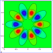
![]() Spontaneous emission
control in microcavities
Spontaneous emission
control in microcavities
|
|
Various microcavity profiles. They are expected to exhibit
the spontaneous emission control, which allows the thresholdless lasing operation
and/or ultra-high speed light emitting diodes. The spontaneous emission
factor is the key factor; it is inversely proportional to the cavity volume
and should be unity for the ideal performance. We experimentally evaluated
the factor of 0.07 for 3-micron-diam.disk laser. This value is the largest
among so-far reported injection lasers. |

![]() Microdisk lasers and
photonic integration
Microdisk lasers and
photonic integration
|
|
This shows the SEM image of fabricated disk laser of 2
microns in diameter. It is the smallest injection laser diodes ever reported.
It operated at room temperature with record low threshold of 150 microamperes
under cw condition. The lasing wavelength was 1.6 microns. Now we are
integrating electrodes and output waveguides to apply this type of device to
a novel functional photonic circuit. |


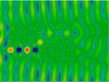
![]() Semiconductor photonic
crystals
Semiconductor photonic
crystals
|
|
|
The concept of photonic crystals has been established
through pioneering works of Prof. Ohtaka of Chiba University, Prof.
Yablonovitch of UCLA, etc. It is a multi-dimensional periodic structure with
the period of half wavelength order. It is expected to achieve the efficient
control of light emission and propagation. We have formed GaInAsP/InP 2D
photonic crystals composed of columns of 200 nm in diameter and 0.6 - 0.8
microns in height. It was formed by EB lithography and CH4-based RIBE or
Cl2-based ICP etching. Peculiar transmission spectra and the polarization
anisotropy in the PL intensity were observed, which can be explained by the
2D photonic band calculation. The light propagation in photonic crystal
waveguides with a sharp bend was also observed at a wavelength range of 1.55
microns. Simulations using the scattering matrix method and the FDTD method
showed a large potentiality of an ultra-small lightwave circuit based on this
waveguide. |


![]() High performance laser
diodes for access networks
High performance laser
diodes for access networks
|
|
|
For access networks, a low cost and high performance LD is
demanded. For this purpose, we have proposed a short cavity LD with deep
grating DBRs. It is formed by a simple dry etching process, which omits the
high reflection coating after the cleavage. A low threshold lasing were
obtained in a 1.55-micron-GaInAsP LD with the grating formed by Cl2 ECR-RIBE,
Theoretically it allows the threshold less than 1 mA and the single mode
operation by a cavity shorter than 50 microns. |


![]() Vertical cavity surface emitting
lasers for 2D array integration
Vertical cavity surface emitting
lasers for 2D array integration
|
|
VCSELs were invented by Prof. Iga of Tokyo Institute of
Technology. After the first achievement of the room temperature cw operation
of his group in 1988, many groups,e.g., J. Jewell, A. Scherer and
colaborators at Bell Labs., had started the research. Even with the long
history over 20 years, the technology of long wavelength VCSELs for fiber communication
has not been established yet. One of the problems is the large heat against
the cw injection. We proposed some heat sinking structures through the FEM
simulation of the operating temperature. |

![]() High resolution active near
field probe based on disk laser
High resolution active near
field probe based on disk laser
|
|
It is difficult to obtain the efficient light output from
whispering gallery mode lasers. However, there exists the evanescent field
spreading to the outer space. We have proposed and demonstrated a novel
active near field probe directly utilizing this evanescent field. The
resolution of the probe was estimated theoretically and experimentally to be
1/10 of the lasing wavelength. We expect that it essentially solves problems
of conventional metal-coated fiber probes, i.e., the low transmission power,
the poor S/N and the difficulty of integration. |
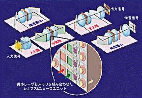
![]() All parallel optical neural
network
All parallel optical neural
network
|
|
|
![]() Micro-electro-mechanical
devices for optical deflection
Micro-electro-mechanical
devices for optical deflection
|
|
Scanned optical beam by micro-mirror |
