![]() Research Review ’00-’02 (2003年3月26日刊行)
Research Review ’00-’02 (2003年3月26日刊行)
Preface
This
is the second research review of Baba Laboratory, which summarizes activities from 2000 to 2002. It also introduces
facilities equipped in between 1994 to 2002.
The first big event in 2000 – 2002 is an international workshop on photonic
crystals (PC) named
In these three years, our research focused on the PC waveguide as a main theme. The
introduction of FE-type EB writer
and ICP etch well improved the
stability and the accuracy of the fabrication process. The experimental results
were well explained by photonic bands obtained by the FDTD method. Still there
remain many issues to be investigated, e.g., reduction in propagation loss,
compatibility to a singlemode fiber, and low reflection and radiation losses at
sharp bends, branches, etc. in a wide spectral range. Also, we addressed the
analyses and the optimum design of light conductive PCs, i.e. superprisms and light deflection devices, high
efficiency interfaces, and third order nonlinear
functions, all of which were the first to be investigated. The PC LED was a simple application to
demonstrate its high efficiency. To suppress the surface recombination in a
highly processed PC made of GaInAsP-InP, we studied some passivation
techniques, and discovered the effectiveness of the methane plasma irradiation. However, for the complete suppression
of such nonradiative effects, we rather employed the surface-grating-type 2D PC. I was happy to find that it could
improve not only the LED efficiency but also those of any
spontaneous-emission-based light emitters. Another important result was the
successful lasing in point defect lasers
at the end of 2002, although it was the fifth achievement in the world and the
result is not included in this research review. All of these results were based
on 2D PCs. We also studied 1D and 3-D PCs. The laser diode with semiconductor
and air distributed Bragg reflectors, which is considered to be a 1D PC,
was improved by using the ICP etch. The smooth etch profile allowed the
demonstration of a clear advantage of this mirror compared with a cleaved
mirror. I was also happy to contribute to
the fabrication of a woodpile 3D crystal lead by RIKEN team. They successfully constructed the crystal by a
micromanipulation technique and observed the photonic bandgap.
During 2000 – 2002, the Priority Area Research and the Research
for the Future of the Ministry of Education, Culture, Sports, Science and
Technology ended, while new big projects CREST
(Prof. Noda, Kyoto Univ., as a leader) of Japan Science and Technology
Corporation, Nanoelectronics Research
Center (Prof. Arakawa, Univ. Tokyo, as a leader), and 21st Century COE program (Prof. Kohno, Yokohama Nat’l Univ., as a
leader) started from 2000, 2002 and 2002, respectively. The continuous grow of
the Japanese activity can also be seen in the number of papers in annual
meetings of the Japan Society of Applied Physics. As program committee members,
I and Dr. Notomi of NTT founded a new session named Photonic Nanostructures and Phenomena. It accumulated many papers,
so the number increased to nearly 70 in 2002, almost twice that in 2000. The
first release of the Technology Roadmap,
which was edited by Prof. Noda, I myself and Dr. Kosaka of NEC, published from
Optoelectronic Industry and Technology Development Association, and distributed
to more than 800 industrial groups, became a powerful driving force for the
development of PCs. Due to the rapid development in these three years, we had
to renew the contents and release the second version in 2002 with additional
editor, Dr. Notomi. I hope this trend is still maintained when the next
research review is planned.
Regarding microdisk lasers, which has been another
main subject of this group, the lasing threshold was steadily reduced within
these three years. In 2000, a lowest
record threshold of 40 microamperes for GaInAsP compound system was
achieved in a 2.7-micron-diameter device by cw current injection at room
temperature. It was attributed to the precisely vertical etching by the ICP
method, which improved the uniform carrier diffusion. The integration of metal pad electrode was realized by using a polymer
cladding. The device not only exhibited the lasing but also the reduction in
thermal resistance and the athermal
effect. An ideal athermal laser, in which the lasing wavelength is
independent of the temperature, is theoretically predicted using a very thin
disk. The cw lasing by photopumping was also obtained for the first time with a
threshold power of 30 microwatts. In
2002. However, this record was easily broken by a microgear cavity to 17 microwatts, which is a microdisk having a
rotationally periodic grating. This threshold is a renewed lowest record for
lasers made of GaInAsP material system. One of the surprising theoretical
discoveries was that the minute control of electric and magnetic field profiles
in the microgear can improve the Q factor of the microdisk. Another unique
characteristic found in these microdisk-type lasers was the strain relaxation phenomenon in the
disk active layer. The lasing wavelength of these lasers often red shifted from
the PL peak wavelength. This suggests the phenomenon, resulting in the
threshold reduction by the drift current flowed from the center region to the
disk edge where the lasing mode is localized. The spontaneous emission factor of over 0.1 was precisely evaluated
from the output - pump characteristic and the wavelength - pump
characteristic. This is one of the
highest value so far reported for semiconductor lasers. Next important issue is
to demonstrate the Purcell factor. It has been partially demonstrated at room
temperature at the end of 2002. The result will be included in the next
research review. As a functional device that utilizes the microdisk is the active near field optical probe. By
putting an object close to a lasing microdisk and scanning the relative
position, the shape of the object or the mode profile of the microdisk laser
was successfully visualized through the change of the lasing power.
A new subject we started studying within these three
years is the Si photonics, which is
based on the Si photonic wire waveguide in an SOI substrate. The pioneering work
was done by MIT and some other groups, but published papers are still very
limited. We focused on this waveguide because the fabrication technique is
similar to that for the PC waveguides, but the design and light propagation
characteristics are much simpler than those of the PC waveguide. We were
surprised at experimental results, which well agreed with 3D FDTD simulations.
The singlemode propagation was observed in a submicron rectangular core. The
Fabry-Perot resonance indicated that the group
index of this waveguide can be much higher than the material index. A sharp bend with a radius of a few mm showed a negligible low bend loss. The polarization
crosstalk was investigated and some optimized bends for a low crosstalk was found
through the FDTD simulation. The bend-waveguide-type
branch exhibited a low excess loss less than 0.3 dB and the Robustness for
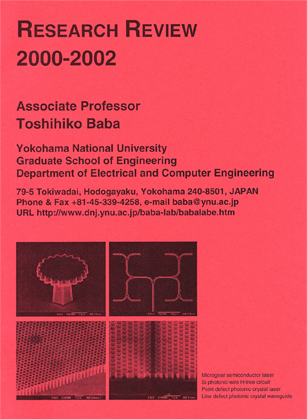
a fabrication error. This branch enabled the successful demonstration of an H-tree optical signal distribution circuit.
Recently, we can feel that this waveguide has attracting almost comparable
attention to that for the PC waveguide. With so developed basic technologies, I
can now expect to demonstrate more sophisticate circuits in the near future.
I wish to acknowledge Prof. Y. Kokubun, Yokohama National
University, Prof. K. Iga, Prof. S. Arai and Prof. F. Koyama, Tokyo Institute of
Technology, Prof. K. Inoue, Hokkaido University, Prof. K. Ohtaka, Chiba
University, Prof. S. Kawakami, Tohoku University, Prof. Y. Aoyagi, RIKEN, Prof.
Y. Arakawa, University of Tokyo, Prof. S. Noda, Kyoto University, and Dr. M.
Notomi, NTT, for their great support of our research and many valuable
suggestions. Also, I would like to thank professors and staffs of the
communication group C of Dept. Electrical and Computer Eng., Yokohama National
University, professors and staffs of Precision and Intelligence Laboratory,
Tokyo Institute of Technology, Dr. A. Kasukawa and other members of Yokohama
Laboratory, The Furukawa Electric, and photonic crystal research members of
NEC, Hitachi, NTT, RIKEN, FESTA, NIMS, etc., for their discussions and
supports. Our work was supported by the Ministry of Education, Culture, Sports,
Science and
Toshihiko
Baba, Associate Professor
(少量,在庫があります.欲しい方は電子メールで連絡してください.)